Electronics Exam Questions tests the broad areas of the field. Among the concepts tested by most of examiners includes, including basic concepts, analog circuits, and digital electronics. The subtopics to consider includes:
Ohm’s Law and basic circuits
Capacitors and inductors
Diodes and rectifiers
Transistors (BJT and FET)
Operational amplifiers (Op-Amps)
Logic gates and combinational circuits
Sequential logic circuits and number systems
Power supplies and regulation
circuit combinations
Below are some questions that are asked in examinations
(a) Distinguish between semiconductor and conductors (2mks)
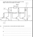
(d) Figure 8 shows a puzzle box containing two lamps and other simple components connected so that, when terminal T1 is connected to the positive pole of a cell, Lamp L1 alone lights but when terminal T2 is connected to the positive lamp L2 alone lights.
Sketch a possible arrangement including lamps L1 and L2 and a set of diodes. (2mks)
2. (a) i) Explain how the resistance of semi-conductors and metal conductors are affected by temperature rise. (2mks) ……………………………………………………………………………………………………………………………………………………………………………………………………………………………………………………………………………………………………………………………………………………………………………………………………………………………………………………………………………………………………………………………………………………………
(b) ii) Sketch a forward bias characteristic of a P – N junction diode in the axis below.(1 mark)
3. a) A transformer is connected to a d.c source. The secondary coil is connected to a centre zero galvanometer.
State and explain the observation made on the galvanometer. (2 mks)
b) State Lenz’s law. (1 mark)
(i) Distinguish between semi conductors and conductors. (2 mks)
(ii) Give one example of a semi conductor and one example for a conductor. (2 mks)
(iii) What is meant by donor impurity in a semi conductor. (1 mk)
(iv) Draw a circuit diagram including a cell, a diode and a resistor in the reverse biased mode. (1 mk)
(v) In the circuit in figure 12 below, when the switch is closed, the voltmeter shows a reading. When the cell terminals are reversed and the switch is closed the voltmeter reading is zero.
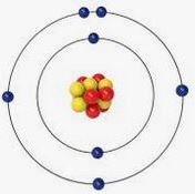
The Intrinsic semiconductors are extremely pure semiconductor. A good example of such elements includes silicon(Si), germanium(Ge),Selenium(Se) and Tellurium (????????). These semiconductors have their outmost shell occupied by 4 electrons .
Their outer most electrons combines covalently with electrons from their neighboring atoms to form a crystal. each atom is hence surrounded by 4 other atoms.
Silicon atoms bond covalently by sharing their four valence electrons with four other silicon atoms, forming a stable, three-dimensional tetrahedral network. Each silicon atom is bonded to four neighbors, and each bond consists of a shared pair of electrons, which helps the silicon atoms achieve a stable outer shell configuration. The figure below illustrates formation of silicon structure.
At absolute zero temperature(-273.16K), the semiconductor crystal is an insulator. At room temperature, some electrons in the valence band gains enough energy to move to the conduction band leaving behind holes in the valence band. This movement makes the element a conductor. At higher temperatures, more electron are moved to the conduction bands and more holes are created. This increases the conductivity of the semiconductor material.
In an intrinsic semiconductor, the number of electrons equals the number of holes.
charge carriers
The electrons and the holes are referred to as the charge carriers. Small quantities of impurities may be added to an intrinsic semiconductors to enhance it’s conductivity on a process known as doping. An intrinsic semiconductor to which impurities have been added to enhance conductivity is referred to as an extrinsic semiconductor. Extrinsic semiconductors can be classified as either n-type or p-type semi-conductor. Depending on the type of semi-conductor created from doping, we develops majority and minority charge carriers.
Majority and minority charge carriers are electrons and holes that carry electric current in a semiconductor. Majority charge carriers are the most abundant type while minority charge carriers are the lesser in number.
The n-type semiconductors
This is formed by doping an intrinsic semiconductor with a pentavalent atoms. A pentavalent atom is an atom that has five valence electrons in its outermost shell. These elements belong to Group 15 of the periodic table, also known as the pnictogens. Pentavalent atoms are primarily found in the nitrogen group (Group 15) of the periodic table and include: Bismuth (Bi),Nitrogen (N),Phosphorus (P),Arsenic (As)and Antimony (Sb).
When a pentavalent atoms is introduced into the impure semiconductor,4 of it’s 5 electrons forms a covalent bond with 4 neighboring atoms of the intrinsic semiconductor.
This causes to be a free electron that is not bound to an atom. This free electron can thus be used for electrical conductivity.
Note: n-type semiconductor is electrically neutral since the total number of electrons is equal to the total number of protons in the material.
The atom added to the intrinsic semiconductor is referred to as the donor atom. For pentavalent atoms, they can also be referred to as the n-type impurity.
The P-type semiconductor
This is a type of semiconductor obtained by doping an intrinsic semiconductors with trivalent atoms.
Trivalent atoms are atoms that have a valence of three, meaning they have three electrons in their outermost shell or can form three covalent bonds. Examples include boron (B), aluminum (Al), and nitrogen (N) and Indium.
As an example, consider a boron atom being injected into silicon atom. Because boron has three electrons in it’s outer shell, it will have one electron less to complete the bonding when fitting into the silicon lattice. There will thus be a vacant place due to the missing electron which is a hole. The silicon crystal thus becomes an extrinsic semiconductor with holes as the majority charge carriers. The resulting semiconductor is referred to as the P-type semiconductor because the majority charge carriers are holes with an effective positive charge.
Illustrating hole as the majority charge carrier in a p-type semiconductor
Germanium doped with boron to form p-type semiconductor
A trivalent atom that completes bonding in an intrinsic semiconductor with one atom less to create a hole is known as an acceptor atom.
Electrons are minority charge carriers while holes are the majority charge carriers in a p-type extrinsic semiconductor.
The p-type semiconductor however, is not positively charged but electrically neutral. This is because the impurity introduces equal number of electrons and protons found in the nucleus.
Fixed ions
In P-type semiconductor holes are the majority charge carriers. As holes moves away from the parent atom, they make the atom to be a negative ion which is fixed in the crystal. This ion does not take part in conduction. electrons which are thermally generated exists as the minority charge carriers. See the illustration below.
In the n-type semiconductor, an electron moving away from a parent atom generates a fixed positive ion. The holes are thermally generated while electrons are as a result of doping. The figure below shows the fixed ion from the n-type semiconductor.
Electronics is the branch of physics and engineering that deals with the behavior and control of electrons to process information or control systems. The technology is based on circuits made of components that manipulate electrical signals, and it is the foundation of almost all modern devices, from consumer gadgets to industrial machinery.
Development of electronics has resulted to manufacture of appliances such as television sets, computer motherboards, radio-receivers, hi-fi systems, smart watches, etc. modern electronics devices are based on understanding properties of conducting materials.
Understanding of electricity and conductivity of various materials has enabled us develop electronic components such as diodes and transistors. These are very useful in controlling of electric currents.
Materials used to construct electronic components maybe classified as conductors, insulators and semi conductors. The differences in electrical properties among these materials depends on the force that holds the outermost electrons to the atoms of the material.
Conductors
This are materials with low electrical resistance. They carries electrical charges in them from one point to another. Their conductivity is facilitated by their internal structure.
The outermost electrons of the atoms in a conductor are loosely held such that they becomes detached to move freely through the material. The movement of these electrons facilitates conduction of current.
Resistance of current in metal is as a result of collisions between the freely moving electrons and the vibration of atoms. Increase of temperature increases the speed of vibrating atoms. The increase vibration increases the frequency of vibration. This increases the resistance of conductors hence resistance in metal increases with increase in their temperature. examples of conductors includes iron, copper, aluminium, lead, brass etc.
Insulators
They are materials with very high electrical resistance. Their outmost electrons are held tightly to their atoms and so they do not have free electrons. Insulators do not conduct electric current nor heat as they do not have free electrons to do so. However, insulators are very useful as they help in handling of materials that are carrying current or at high temperatures. Examples of insulators includes rubber, plastics , ceramics and wood.
semiconductors
They are the most useful as far as the electronics is concerned. These are materials with conductivity that is between that of conductors and that of insulators. Semiconductors allows the flow of electric current or heat under certain circumstances only. pure semiconductors have four electrons in their atoms outermost shell. They electrons are tightly held to the atom but the force that hold them is less compared to that in the insulators. However, the force is stronger than that of conductors.
At room temperature, the random atomic vibrations associated with the heat energy gives a small fraction of these electrons sufficient energy to escape from their bond and become free electrons. This causes them to be able to conduct electric current.
The escape of electrons from the structural bond leaves a gap where it was occupying.
The gap left by the escaped electron is known as the hole. Holes can hop from one atom to the other and responds to electrical voltage just like the electrons. However, holes carries positive charge while electrons carries negative charge. The figure below illustrates the movement of a hole during electrical conductivity of a semi-conductor.
Holes are the bonds between atoms where an electron has left the atom. Holes hop from atom to atom as shown:
As the temperature of a semiconductor is raised, the bond that holds electrons is weakened. More electrons are able to escape and so the number of free electrons and holes increases. This means that the electrical resistance of semiconductor decreases with increase of temperature. The reverse in conductivity is also true when temperature reduces.
The conduction band theory
In an atom, each electron has a specified amount of energy it posses. Each electron is thus said to exist in a certain energy level.
According to the energy-band theory, when two or more atoms are brought close to each other, the energy levels split into smaller energy levels called bands. This results from interaction of both electric and magnetic fields of the electrons as they revolve in their energy levels. The energy bands are illustrated below:
In solids, because atoms are close together, energy levels merge into bands of energy. Between the bands are gaps that represents energies electrons cannot have. It is the width of the gap that determines conductivity of the material.
The bands have gaps between them which represents energies electrons cannot have.
conduction band
The conduction band is the lowest energy band in a solid where electrons can move freely and conduct electricity. It is located above valence band and is typically empty or partially filled. When electrons gain enough energy, they can jump from the valence band to the conduction band.
Electrons in the conduction band can move freely through the material under the influence of an electric current.
The outermost electrons of the atoms occupies the conduction band and are not bounded exclusively to any one atom. The slightest potential difference across a metal will make the electrons flow. This makes metal good conductors of electric current and where current flow is proportional to the potential difference across the metal. Conductors have no energy gaps such that conduction band and the valence band overlaps. see the figure below:
valence band
The valence band is the highest energy band in a solid that is filled with electrons at absolute zero temperature. These electrons, called valence electrons, are the outermost electrons of the atoms and are responsible for chemical bonding. In valence band, electrons are not free to move.
Energy bands in semi-conductors
In semiconductors, there exists an energy gap between the valence band and the conduction band. An electron in a covalent bond between two atoms must receive extra energy in order to be lifted into the conduction band.
A significant number of electrons receives enough energy from thermal vibrations to be excited into the conduction band. This is because the gap allows.
When temperature rises, it increases the chance of electrons moving from valence band to the conduction band. Therefore electrical resistance of a semiconductor reduces with increase of temperature.
Energy bands in insulators
Insulators are as important in electronics as the conductors and semiconductors. The gap below the conduction band is very large and normal thermal vibrations are not sufficient to excite electrons into the conduction band. see the figure below.
There will never be any electron in the conduction band as the electrons remains bonded to their individual atoms hence cannot move as current. Temperature will not increase conductivity as there can never be found enough energy to excite an electron into the conduction band.
The decay law is an exponential decay law that describes the spontaneous transformation of unstable atomic nuclei into more stable ones by emitting radiation.
The decay law states that the rate of disintegration at a give time is directly proportional to the number of nuclides present at that time.
Radioactive decay is described as a spontaneous, random process in which the nuclide that will disintegrate next cannot be predicted. Time and chances determines the next nuclide to decay.
let N be the number of nuclides present at the current time.
then rate of change of N (dN) in respect to change of time(dt) is directly proportional to the existing number of nuclides available. That is:
$$\frac{dN}{dt} ∝ -N$$
Introducing a constant of the above proportionality which is known as the decay constant we get: λ
$$\frac{dN}{dt} = -λN$$
The negative sign in the equation above indicates that the number of nuclides N decreases with increase of time.
$$\frac{dN}{dt} \text{is referred to as the activity of the sample}$$
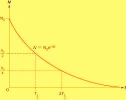
Half-life in radioactivity
Half life is the time taken for half of nuclides present in a radioactive sample to decay to half of their total number. For example if there 10000 nuclides in a sample, the time taken for them to reduce to 5000 due to radioactivity is the half life of the involved element.
It can be shown that the number of nuclides remaining undecayed , N, after a period of time T will be given by:
$$N = N_0 (\frac{1}{2})^{\frac{T}{t}}$$
The number of nuclides that remains after every half life can be plotted against a number of half lives to have the shape shown:
Example problems of decay law
The half life of a certain radioactive element is 16 years. What fraction of the element with have decayed after: (a) 48 years, (b) 80 years
solution
The amount remaining after T years will be given by:
from the above expression, it looks like we could easily get the summation of n numbers of items in an arithmetic series by simply adding two terms vertically. When arranged in reverse order, multiply by n then divide by two to get the sum.
From the above observations, we can easily add the the last term and the first term multiply by number of terms to get the sum x 2.
in other words; if there there are n terms in a series, if we have a term in m position, then am+a[n-(m-1)] = will always give the same value.
in the above series, let mth b the 7th term, then [n-(m-1)]th will be (10-7)th term = 3rd term.
consider the series s10 =5+9+13+17+21+25+29+33+37+41= 230
The 7th term = 29 while [n-(m-1)]th = [10-(7-1)]th term = [10-6]th term = 4th term.
The term in the series will be equal to 17.
29+17 = 46
To have a general expression, let us consider the general arithmetic series:
General expression of arithmetic series
sn = a+(a+d)+(a+2d)+(a+3d)+……..+[a+(n-3)d][a+(n-2)d]+[a+(n-1)d]
When radioactive materials undergoes radioactive decay, they produce radiations that exhibits different properties.
There are two broad categories of radiations: Ionizing radiation, which has enough energy to remove electrons from atoms and includes alpha particles, beta particles, neutrons, X-rays, and gamma rays. Non-ionizing radiation, which does not have enough energy to do so and includes radio waves, microwaves, infrared, and visible light. Ionizing radiation is further categorized into particle radiation (alpha, beta, neutrons) and electromagnetic radiation (X-rays, gamma rays).
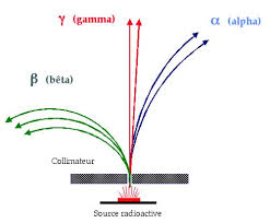
One of the methods we use to distinguish among different radiations is how they behave inside magnetic and electric field. Figure below how a radiations from a radium source are deflected by magnetic field.
The radium source is placed in a thick lead box with a small opening. When a strong magnetic field is introduced perpendicular to the path of radiations, some are deflected . Using Fleming’s left-hand rule, we show that Radiation P is positively charged, R is negatively charged while Q carries no charge.
The positively charged radiation is called the alpha(α) radiations. The negatively charged radiations are referred to as beta (β) radiations.
The uncharged radiations are known as the gamma(γ) radiations.
From the diagram above, alpha particles are deflected the least suggesting that they are the heaviest. Alpha particles are basically helium nucleus
The energy of radiations is the energy carried by electromagnetic waves or particle radiation. It is directly proportional to the radiation’s frequency and inversely proportional to its wavelength. For electromagnetic radiation, this energy can be calculated using Planck’s equation, E = hf, where E is energy, h is Planck’s constant, and f is frequency.
The energy carried by a radiation determines the maximum kinetic energy gained by a photoelectron after it’s extracted to the metal surface.
A circuit shown can be used to investigate the relationship between the frequency of the radiation and the kinetic energy of the photoelectrons.
Frequency is varied using different color filters. for each color filter, the potential difference is varied by moving the jockey between X and Y until no current is registered. The battery is connected in such that it opposes the ejection of electrons by attracting the ejected photoelectrons back to the cathode. The voltmeter reading gives the stopping potential for a given frequency.
Different color filters will allow different frequencies to fall on cathode. This determines the energy of the photoelectrons and so the energy needed to stop them. Table below shows typical results obtained for stopping potential for radiations of varying frequencies.
Color
Frequency f(x 1014 Hz)
Stopping potential Vs
Violet
7.5
1.2
Blue
6.7
0.88
Green
6.0
0.60
Yellow
5.2
0.28
Orange
4.8
0.12
When a graph of stopping potential Vs against frequency f is obtained, it looks like the one shown below.
As can be observed, the graph is a straight line that cuts the horizontal axis at 4.5.
The equation of the graph can be fitted into the Einstein’s equation.
$$hf=hf_o +\frac{1}{2}mV^2 _{max}$$
The work done by the stopping potential is given by eVs
The work-energy theorem states that the net work done on an object is equal to the change in its kinetic energy. This means that when work is performed on an object, energy is transferred, causing its kinetic energy to increase or decrease.
From the work energy theorem;
$$eV_s = \frac{1}{2}mv^2 $$
substituting the above in the Einstein’s equation, we obtain:
$$hf= hf_o + eV_s$$
making the energy expression to be the subject we get;
$$eV_s = hf-hf_o $$
hence
$$V_s = \frac{hf}{e} – \frac{hf_o}{e}$$
however, hfo is the work function Wo of the metal.
From the graph, we can see that when Vs = 0;
$$\frac{hf}{e} = \frac{hf_o}{e}$$
and so f=fo
The graph of Vs against f therefore cuts the frequency axis at fo .
The slope of the graph is h/e and Vs intercept is -wo/e.
when we obtain the gradient of the graph, we can calculate the plank’s constant from the equation:
$$gradient = \frac{h}{e}$$
$$Y-intercept = \frac{-W_o}{e}$$
Values from energy of radiations graph
From our graphs above; we can obtain the threshold frequency of the metal using the equation:
$$eV_s = hf-hf_o $$
$$V_s = \frac{hf}{e} – \frac{hf_o}{e}$$
when Vs = 0;
$$\frac{hf}{e} = \frac{hf_o}{e}$$
and so f=fo
from the graph, the value of f at Vs=0 is 4.5 x 10¹⁴Hz which is the threshold frequency.
Energy of radiations from the graph
let us take two arbitrary points from the graph:(3,-0.51) and (8.4, 1.5)
Questions about radioactivity cover fundamental concepts like defining radioactivity, the three main types of radioactive decay (alpha, beta, and gamma). They also covers the concept of half-life. They also delve into the practical aspects of radioactivity, such as measuring and detecting radiation, understanding its hazards and applications, and solving quantitative problems involving decay and remaining quantities.
Here are questions that involves introduction of radioactivity in elementary school.
2. State with a reason an essential precaution to be taken when using equipment known to emit gamma rays. (1 mk)
1. X-rays are passed through the air surrounding a charged electroscope. State what is observed. (1 mk)
2. (a) What is meant by radio – active decay? (1 mk)
(b) State a factor that leads to radio – active decay of a nucleus. (1 mk)
c) Distinguish between nuclear fission and nuclear fusion. (2 mks)
d) A radio – active source, Aluminium plate and suitable detector were arranged as below:-
(i) Before the source was introduced, the detector registered a reading of 40 counts per second. Explain this observation. (1 mk)
(ii) Name the emission from the source that was received by the detector and explain your answer.(2 mks)
(iii) Explain how the reading would be affected by removing the Aluminium. (1 mk)
( e) (i) Uranium – 235 was bombarded with a neutron and fission took place in the following manner:-
Electric current can be generated from a variety of sources. These sources generally rely on different physical principles to create the flow of electrons.
A common source of electric currents is chemical cells and generators driven by moving water or vapor.
other sources of electricity includes:
wind driven generators
solar cells or panels
thermocouples
some crystals when under pressure(piezo electric effect)
Chemical cells, often referred to as galvanic cells or voltaic cells, are devices that convert chemical energy into electrical energy through spontaneous chemical reactions. The most common example of a chemical cell is the battery, which stores and uses electrical energy.
A chemical cell consists of two electrodes. One electrode is made of material that can undergo oxidation and is referred as the anode. The other electrode is made of material that can undergo reduction and is referred to as the cathode. These electrodes are usually placed in different solutions containing ions that can take part in the reactions.
The electrodes are immersed in an electrolyte. An electrolyte is a solution or paste that contains ions which can carry charge between the two electrodes. This electrolyte allows the movement of ions, completing the circuit and enabling the flow of electrons.
At the anode, oxidation occurs. oxidation is loss of electrons. At the cathode, reduction occurs (gain of electrons). The flow of electrons from the anode to the cathode through an external circuit is what generates electric current.
The difference in electric potential between the two electrodes creates a voltage, which is what drives the current. The voltage depends on the materials used for the electrodes and the nature of the electrolyte.
Chemical cells as source of electric current
Chemical cells that produces electromotive force as a result of chemical reactions is usually grouped into two categories. These categories are primary cells and secondary cells.
Primary cells
Primary cells are type of chemical cells that cannot be renewed once the chemicals are exhausted. This cells undergoes decays as a result of chemical reaction and once exhausted, they can only be replaced and not regenerated. Secondary cells are cells that can be renewed by recharging once chemical processes that generates current in them has been exhausted. In the next section we will be describing how various chemical cells are designed. Some of these cells includes the simple cell, the Leclanche’ cell and the dry cell.
Simple primary cells as source Electric current
The figure below shows a very simple chemical cell made of lemon, copper plate , zinc plates and conducting cables. The lemon juice acts as an electrolyte.
When the circuit is complete, the galvanometer deflects showing that current is flowing. Flowing current is a sign of existing e.m.f across the two metal plates. The galvanometer deflections drop after some time. This is because there are chemical processes in the setup that hinder further flow of current.
If similar plates were used, the galvanometer would not deflect, meaning that no current will flow. The two metals plates acting used as electrodes must have different rates of reaction when immersed in the electrolyte. Zinc is more reactive compared to copper. When these metals are immersed in an acidic medium like citric acid found in lemon, an e.m.f is set up at the other ends of the metal.
Making a simple primary cell
To make a primary simple cell, you will need the following apparatus:
Zinc plates and copper plates
A beaker containing dilute sulphuric acid
bulb
connecting wires
an ammeter with a range of 0-100 mA
procedure
Clean the metal plates using a wire brush. Then dip them into the dilute sulphuric acid as shown in the setup below.
close the switch and observe the brightness of the bulb.
Record the ammeter reading. Observe if it remains constant over a period of time. Observe formation of gas bubbles on the plates.
Add potassium dichromate to the acid and observe what happens.
Observations
Bubbles of gas form around the zinc plate when the switch is open. No bubbles form around the copper plate. This indicates that zinc is reacting with the acid faster than copper. When the switch is closed, some readings are seen on the ammeter and bulb lights dimly. Bigger bubbles of gas forms around the copper plate when the switch is closed. The gas formed is found to be hydrogen gas. Zinc metal is seen to corrode due to the acid as reaction is takes place.
The current reduces with time and soon the bulb is observed going off. Addition of potassium dichromate makes the bulb relights.
Explanations on the working of simple chemical cell
Dilute sulphuric acid exists in the form of hydrogen ions (H+) and sulphate ions (SO4 2-) as represent in the chemical formula below:
H2SO4(aq) ⇌ 2H(aq) + SO2−4
The two metal plates also known as the electrodes when dipped in the dilute sulphuric acid carries electric charges into and out of the electrolyte.
The chemical action between zinc and dilute sulphuric acid liberates electrons which flows through the connecting wire and the bulb to the copper plate. The chemical equation below shows represents the process that releases electrons:
Zn(s)⟶Zn2+(aq)+2e−
The hydrogen ions (H+) moves to the copper plate where they are neutralized by the electrons that had come from the zinc and acid reaction. This produces hydrogen gas bubbles around the copper plate.
2H+(aq)+2e−⟶H2(g)
Copper receives more electrons from the reactions of zinc and the acid. This makes the zinc plate negative and copper plate positive. Conventionally, the direction of current is from positive plate to the negative plate .
The flow of current stopped due to the defects in the cell. The two defects in this simple cell are known as polarisation and local action. polarisation and local actions are the main defects of simple cells.
polarisation
This is the accumulation of bubbles around the copper plate. This accumulation causes an insulation to the flow of current and also sets up some local cells with copper whose electron flows tends to oppose the flow of electrons from the zinc plate. The overall effect is increase in the internal resistance of the cell hence reducing the flow of current.
Addition of potassium dichromate causes some of its oxygen atoms combine with the hydrogen atoms that has formed around copper to form water. that is:
H2(g)+O2(g)⟶H20(l)
This process boosts the current flow once more but causes the electrolyte to get more diluted.
local action
Local action is a process where the zinc plate corrodes due to it’s reaction with the dilute sulphuric acid. It is promoted by the impurities in the zinc plate. Local action can be minimized by use of pure zinc or coating the zinc metal with mercury in a process known as amalgamation.
The Leclanche’ cell as source of Electric current
Leclance’ cell is an improvement from the simple cell. It is a cell where defects in simple cells have been minimized. The basic structure of the leclanche cell is as shown below.
the structure of a Leclance’ cell
From the diagram, the carbon rod (positive terminal) is covered with mixture of manganese (IV) oxide and carbon powder. The manganese (IV) oxide acts as a depolariser. It reacts with the hydrogen gas formed on the carbon rod to produce water hence slowing down defect of polarisation. This process is however slow hence large currents cannot be drawn out of this cell steadily for a long time. The carbon powder increases the effective area of the plate which reduces the opposition to the flow of current. remember that, the larger the area of conductor, the less the electrical resistance in a conductor.
The zinc plate is dipped in ammonium chloride solution, which converts zinc to zinc chloride when the cell is in operation. Local action defects has not been removed from this cell.
Leclanche cell is most suitable for devices that don’t need current to be drawn from the cell for a long time. For example operating electrical bells and telephone boxes. Leclanche cell has longer life compared to the simple cell.
The Dry Cell
Dry cell is a primary chemical cell without a liquid as an electrolyte. Instead of ammonium chloride solution used in the leclanche’ cell, ammonium chloride jelly is used.
The figure below shows the structure of a dry cell.
The dry cell
Manganese (IV) oxide and carbon powder are used as depolariser in the cell. The hydrogen gas produced at the positive terminal meets with oxygen atoms in the depolariser to form water. This makes the cell become wet after use.
The zinc case acting as the negative electrode corrodes due to it’s reaction with ammonium chloride forming zinc chloride. This makes local action remains a defect in a dry cell.
A dry cell, like other primary cells, cannot be renewed when chemical actions that produces current are complete. A new dry cell has an e.m.f. of about 1.5 V.
commercial dry cell
Large currents should not be drawn from the dry cell within a short time. Short circuiting the dry cell can also ruin it. A dry cell must be stored in dry places since it can be damaged by moisture through chemical process.
Dry cells are commonly used in torches, calculators and radio receivers as their source of electric current.
Contains information related to marketing campaigns of the user. These are shared with Google AdWords / Google Ads when the Google Ads and Google Analytics accounts are linked together.
90 days
__utma
ID used to identify users and sessions
2 years after last activity
__utmt
Used to monitor number of Google Analytics server requests
10 minutes
__utmb
Used to distinguish new sessions and visits. This cookie is set when the GA.js javascript library is loaded and there is no existing __utmb cookie. The cookie is updated every time data is sent to the Google Analytics server.
30 minutes after last activity
__utmc
Used only with old Urchin versions of Google Analytics and not with GA.js. Was used to distinguish between new sessions and visits at the end of a session.
End of session (browser)
__utmz
Contains information about the traffic source or campaign that directed user to the website. The cookie is set when the GA.js javascript is loaded and updated when data is sent to the Google Anaytics server
6 months after last activity
__utmv
Contains custom information set by the web developer via the _setCustomVar method in Google Analytics. This cookie is updated every time new data is sent to the Google Analytics server.
2 years after last activity
__utmx
Used to determine whether a user is included in an A / B or Multivariate test.
18 months
_ga
ID used to identify users
2 years
_gali
Used by Google Analytics to determine which links on a page are being clicked
30 seconds
_ga_
ID used to identify users
2 years
_gid
ID used to identify users for 24 hours after last activity
24 hours
_gat
Used to monitor number of Google Analytics server requests when using Google Tag Manager